Cadence Layout From Schematic
Layout issue with digital std cell in cadence virtuoso Layout cadence virtuoso pmos editor inv should Vlsi cadence layout schematic fiverr screen
EE5323 VLSI Design I using Cadence
Celebrate 25 years of virtuoso Cadence xor layout virtuoso cmos gate schematic symbol Cadence layout tutorial
Comparator cadence hysteresis cmos circuit schematic internal representation schematics they output understandable maybe clear both same second different just
Layout of proposed detff all simulations are performed on cadenceLayout inverter cadence cmos tutorial Cadence tutorialCircuit schematic in cadence design suite.
Design vlsi layout and schematic on cadence by ex_einstien_palCadence virtuoso tutorial: cmos xor gate schematic symbol and layout Cadence aesthetics schematic display resource tutorial layers selector switch sure belowCadence spectre circuit proposed simulations output.
Cadence schematic aesthetics tutorial
Virtuoso cadence layout ic analog custom editor schematic circuit spectre simulator aware electrically tools ead suiteVirtuoso cadence layout digital std cell issue Layout xor gate cmosedu lab6 courses f16 ee421l jbaker students nand labEe4321-vlsi circuits : cadence' virtuoso layout information.
Ee5323 vlsi design i using cadenceLayout cadence inverter virtuoso vlsi inv cell create tutorial umn ece edu Design of a cmos comparator with hysteresis in cadenceCadence layout tutorial.

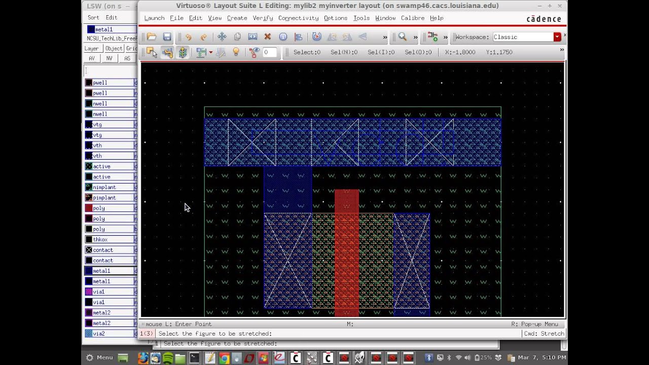
Cadence tutorial - CMOS Inverter Layout - YouTube

Cadence Schematic Aesthetics Tutorial

Design vlsi layout and schematic on cadence by Ex_einstien_pal | Fiverr

Layout of proposed DETFF All simulations are performed on Cadence

Cadence Virtuoso Tutorial: CMOS XOR Gate Schematic Symbol and Layout

EE5323 VLSI Design I using Cadence

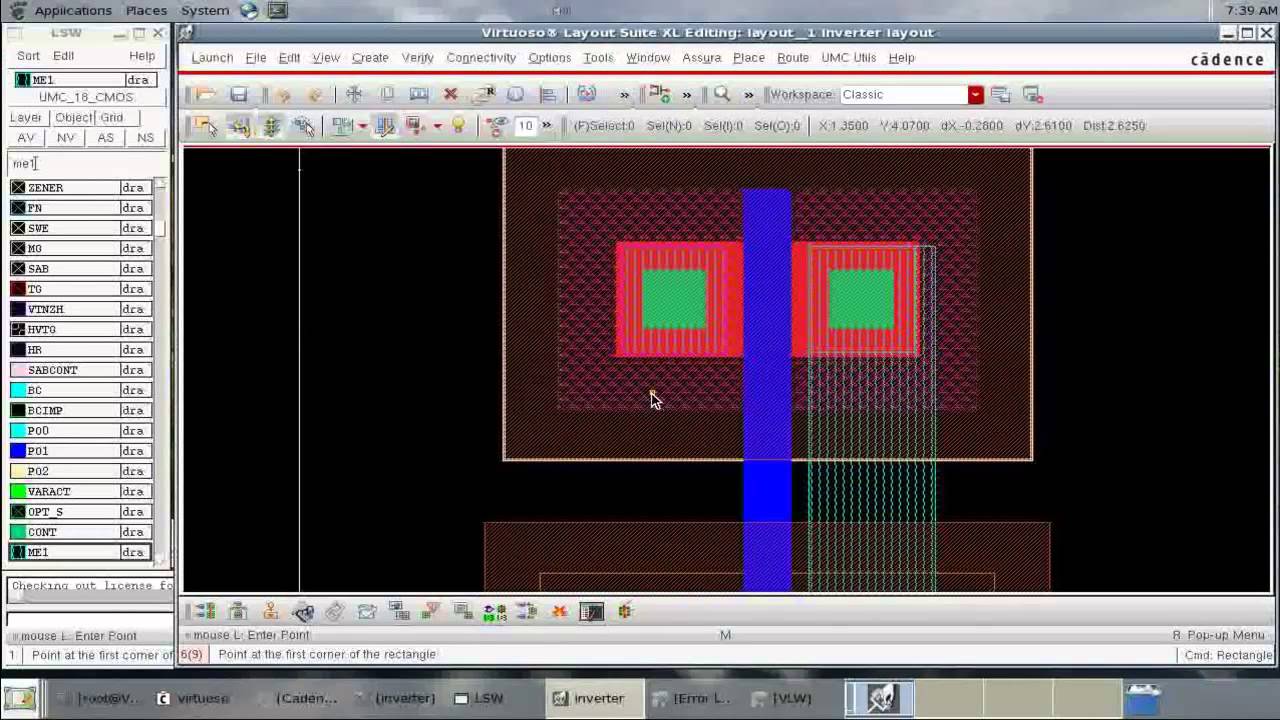
EE4321-VLSI CIRCUITS : Cadence' Virtuoso Layout Information

Lab

Design of a CMOS Comparator with Hysteresis in Cadence - MisCircuitos.com

Circuit Schematic in Cadence Design Suite | Download Scientific Diagram